


PCB Assembly Analysis – Vision, X-Ray, & CT
PCB Analysis using Vision, X-ray, & CT
We combine the strengths of many systems and softwares to offer a broad scope of analysis for our clients. This case study demonstrates how we can use 2D Vision, X-Ray, & CT to analyze PCB assemblies.
We use our programmable, large bed vision system to create automated visual inspection procedures for projects where tactile probing is not feasible. Examples include circuitry, sticker and decal placement, and small, high concentration features like meshes and pin holes. Features can be programmed for just visual accept/ reject of presence.
X-Ray & CT are used to measure internal features – solder joint porosity, fractures, broken wires, failed LEDs, and dimensional analysis if the PCB is complex with housings obscuring the vision system’s line of sight.


Video of Max Resolution Vision Image Transport
This video shows a compiled, max resolution image over 2.5gb. Every zone can be zoomed in on to be analyzed for visual inspection and measurements. Clients use this for a variety of purposes including documentation of condition, dimensional analysis, and visualization of component presence and quality.
You’ll witnessed that the sample piece has two broken components that were caught during visual inspection.
Programmable Feature Extraction
Features like lines, circles, and other geometry can be programmed for automated and repeatable measurement routines. Using PC-DMIS, these features can then calculate GD&T controls like parallelism, straightness, position, and profile of a line. Features can also be exported into .step or polylines for reverse engineering and component rebuild.
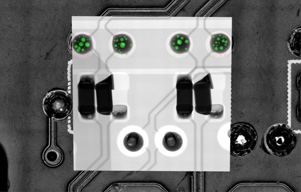
X-Ray for Solder Joint Porosity
Solder joint porosity can be calculated and graded per client specifications. This is particularly useful when clients are making process adjustments, or need to understand how other forms of testing are affecting a known-good/ passing part. For example, if you don’t have documented pre-test data, how can you be sure that thermal shock exposure caused the issue?